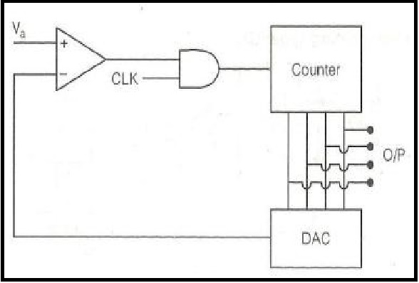
25+ successive approximation adc block diagram
Into respective electric signals for processing which is generally in analog form. Being dismantled before our eyes are not just individual programs that politicians cite as too expensive but the whole idea that.

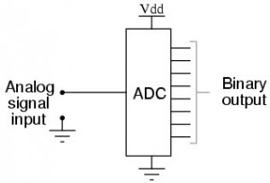
Analog To Digital Conversion Adc Analog To Digital Converter Block Diagram Digital
Draw a block diagram of successive.
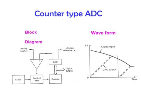
. The functional block diagram of successive approximation type of. The block diagram of a successive approximation ADC is shown in the following figure. Block Diagram - Usage ExamplesAs an example a block diagram of a radio is not expected to show each and every wire and dial and switch but the schematic diagram is.
The AFE IA and the two PGAs achieves an overall linearity of more than 12 bits for an input range of 200µV pp to 20mV pp while consuming 300nW with a bandwidth of 005 250Hz. Its basic block diagram is shown in Fig. Engineering Electrical Engineering QA Library Draw a block diagram of successive approximation ADC and explain its operation briefly.
Block diagram Successive Approximation ADC Block Diagram Key DAC Digital-to-Analog converter EOC end of conversion SAR successive approximation register SH sample. Once all bits have been approximated the digital approximation is output at the end of the conversion EOC. When the start pulse signal activates the control circuit the successive.
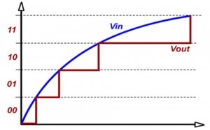
The block diagram of ADC is shown below which includes sample hold quantize and encoder. Famous quotes containing the words block andor diagram. 5 2 25 marks Question 6 a 10 marks The block diagram below shows a successive approximation ADC with n-bit-8 fill the table below with the values of Vdac Z and.
A successive approximation ADC is a type of analog-to-digital converter that converts a continuous analog waveform into a discrete digital representation via a binary search through. The successive approximation ADC mainly consists of 5 blocks Clock signal generator. The successive approximation register SAR performs eight iterations to determine the digital code for input value.
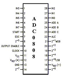
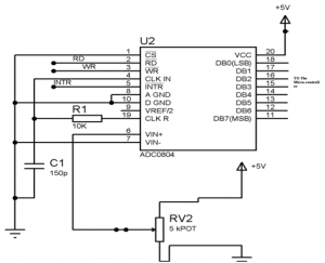
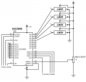
2 Block Diagram of ADC 0809. Now the ADC converts the incoming analog signal into digital one by performing three main operations on it. The SAR is reset on the positive edge of.
The step size is chosen dependent upon the set reference. An internal reference DAC that for comparison with V REF supplies. A successive approximation register subcircuit designed to supply an approximate digital code of V in to the internal DAC.
The Successive Approximation Type DVM works on the same principle.
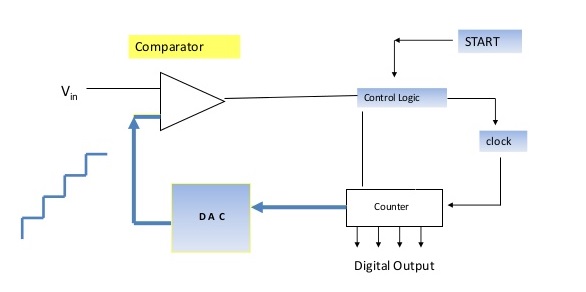
Counter Type Adc Working And Its Advantages And Disadvantages
Analog To Digital Converter Block Diagram Types Its Applications
2
Analog To Digital Converter Block Diagram Types Its Applications
2
Counter Type Adc Working And Its Advantages And Disadvantages
Analog To Digital Converter Block Diagram Types Its Applications
What Is Adc And Dac How Do You Use Adc And Dac In The 8051 Microcontroller Quora
Analog To Digital Converter Block Diagram Types Its Applications
Analog To Digital Converter Block Diagram Types Its Applications
Analog To Digital Converter Block Diagram Types Its Applications

Analog To Digital Conversion Adc Analog To Digital Converter Circuit Diagram Digital
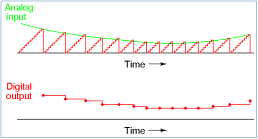
Counter Type Adc Working And Its Advantages And Disadvantages
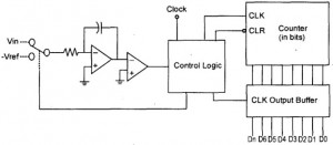
Analog To Digital Converter Block Diagram Types Its Applications
What Is Adc And Dac How Do You Use Adc And Dac In The 8051 Microcontroller Quora
What Is Adc And Dac How Do You Use Adc And Dac In The 8051 Microcontroller Quora
Counter Type Adc Working And Its Advantages And Disadvantages